Architect Labs, a chip-design startup incorporated as Architect Silicon Inc., said on November 18, 2026 that its AI agents had designed a general-purpose CPU called Frostbite. What is new is the AI’s role: in August, the company says, its AI implemented an architecture, or overall chip design, written by two people. This time, the company says, the agents worked out the architecture too. No chip has been made, and the company calls its own power numbers pre-silicon.
According to the company’s post, the agents worked on the compiler, instruction set, microarchitecture, RTL (the code that describes the circuits), verification and final layout for a 7-nanometer manufacturing process. The instruction set lists the chip’s basic commands, the microarchitecture is how its parts carry them out, and the layout is the chip’s physical blueprint.
The company claims 4.59 times the performance per watt, or work done for each watt of power, of one core of a “modern, silicon-proven” conventional CPU. On the 15 test programs the agents never tuned on, the figure is 3.83x. The company says it cannot name the baseline CPU “for legal reasons”.
A CPU based on a 1990 idea
Frostbite is based on interaction nets, a model of computation that Yves Lafont presented at the POPL programming-languages conference in 1990. A program is a network of nodes, and computing means rewriting connected pairs of them. Pending rewrites touch only nearby nodes and never overlap, so they can happen in any order, or all at once, with the same result.
A conventional CPU spends chip area and power tracking which instructions depend on which as a program runs. Architect Labs argues that interaction nets keep those dependencies explicit, so data can live in small memories next to the circuits that use it.
The idea predates the company, and its post cites some of the earlier work. Frostbite programs are written in Vine, an open-source language that compiles to interaction nets through Ivy, an intermediate format from the same project.
Tendrils, a startup whose website carries the line “$30M Raised to Redo the CPU”, is building its own interaction-net processor. Its April 26 explainer, which Architect Labs recommends, presents Vine as a language Tendrils created. A separate open-source project, Lamagraph, has had an interaction-net processor for FPGAs (reprogrammable chips) on GitHub since August 2024.
How the agents worked
The team chose 25 test programs: 10 for the agents to tune on (the search set) and 15 held back for the final evaluation. The 15 include five practical jobs added later, such as LZ4 decompression (unpacking compressed data).
The agents read papers and benchmarks, built Python models to compare architecture ideas, and narrowed them to one concept. The company deleted that phase’s 141-page design document after the first round of RTL: many of its numbers were far from what was physically possible.
“Frostbite was designed with zero architectural priors,” the post says. The company’s About page, however, says that in its process “human architects set the intent and direction.”
From then on, the specification was a set of contracts, formal rules that software can check, written in ASL, the company’s own language. ASL translates to Lean, a math proof checker that Google’s agents also used this month to prove quantum programs correct. The post says Frostbite’s contracts ended up at more than 800,000 lines of Lean.
Arcmodel, a software model of the chip, ran about 200 times faster than an RTL simulation. Its early power and performance estimates were off by almost 250% in the worst case. An automated loop recalibrated it against the RTL until the two agreed within 5%.
Swarms of agents then proposed changes in parallel copies of the code. Each change was checked against the contracts, modeled, implemented and measured, then kept or dropped. In all, the swarm tried 58 ideas and kept 37.
Frostbite has no central scheduler handing out work: each tile, one of the chip’s small processing blocks, handles its own work first. When it has none, it takes spare work from a neighbor, or goes idle to save power if no neighbor has any. “This behavior was never specified by any human,” the post says.
The numbers and what they compare
In synthesis, the step that turns the RTL into logic gates, the design met timing at 800 MHz, meaning the tools found its circuits fast enough for that clock. In the final layout, the figure was 500 MHz.
One Frostbite quad, a two-by-two grid of tiles plus four L3 nodes (third-level memory blocks), takes 0.792 mm². The baseline core, which the company calls TCPU, takes 0.895 mm² on the same process, so the two are of similar size. That core is dual-issue and in-order: it can start up to two instructions per clock cycle, in program order.
Across all 25 programs, the company puts the quad at 4.59 times the baseline’s performance per watt, as a geometric mean (a standard way to average ratios). The figure is 6.02x on the 10 search-set programs and 3.83x on the 15 held-out ones. Performance per unit of chip area averages 8.77x, a separate measure.
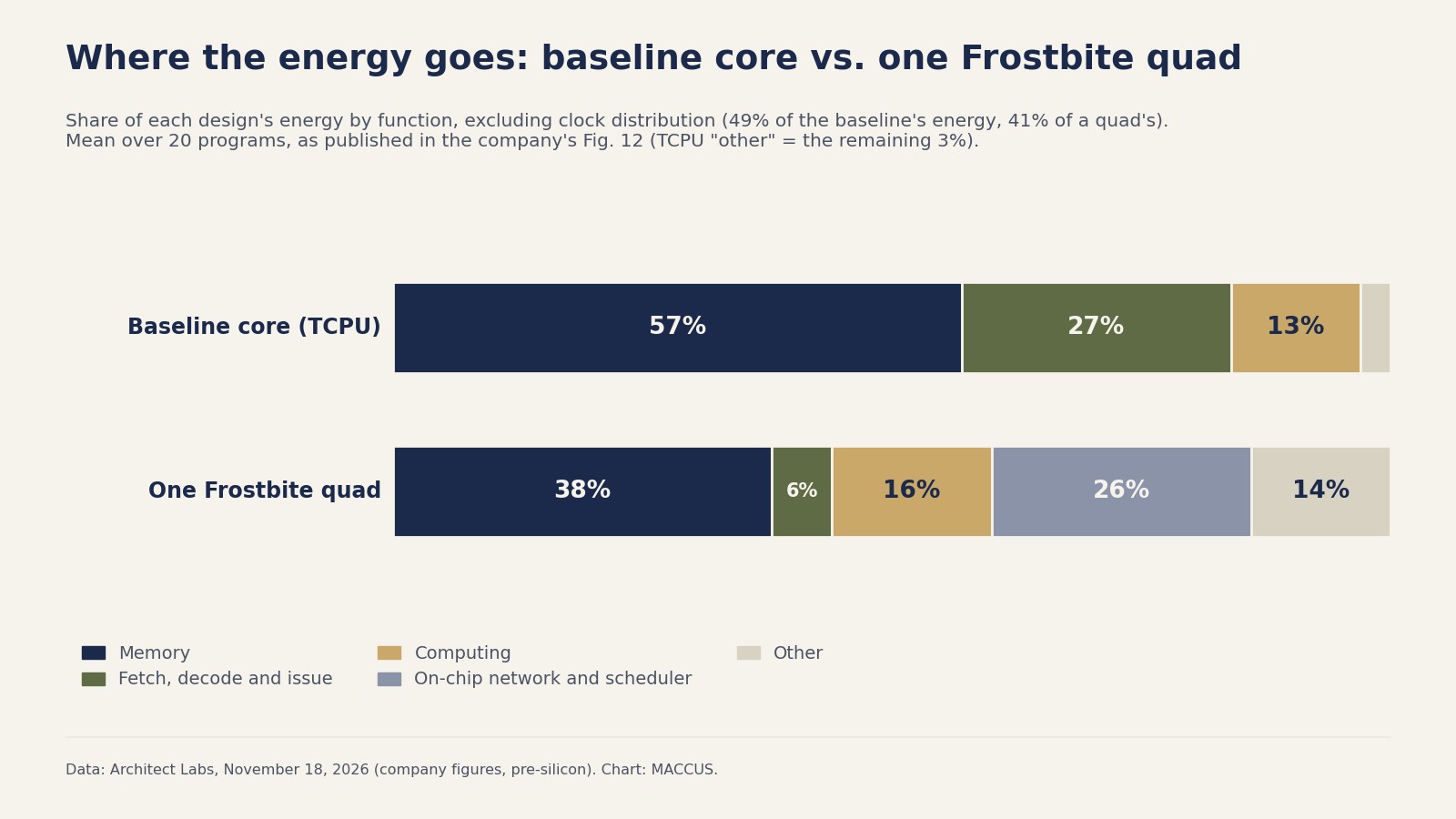
The company’s energy breakdown, averaged over 20 programs, shows where it places the savings. It leaves out the clock network, the wiring that keeps circuits in step, which uses 49% of the baseline’s energy and 41% of a quad’s. Of the rest, the baseline spends 57% on memory and 27% on fetching, decoding and issuing instructions. Frostbite spends 38% on memory and 6% on instructions, but 26% on its on-chip network and scheduler, the cost of moving work between tiles.
Redwood in August
On August 27, Architect Labs announced Redwood, a chip design for running AI models that it said its AI designed, verified and deployed in under two weeks. Two human architects wrote its specification, and a small version runs on an FPGA. The company projected that on Samsung’s 8 nm process, the class used by Nvidia’s Jetson Orin Nano, a small AI computer, Redwood would deliver 3.4 times the performance per watt of a Jetson it measured.
OpenAI’s own chip-design results
OpenAI published its own chip-design results on November 18, including the AMD GPU gains covered here on November 19. On November 3, it had described two staff members using its GPT-6 Astra model to design a device in under a week.
One test in the November 18 post used PicoRV32 and Ibex, two open-source processor cores based on the open-standard RISC-V instruction set. All five OpenAI models scored higher when they designed a core from written requirements than when they tried to improve the existing design. OpenAI adds its own caveat: starting from requirements let the models leave out features of the original cores, such as performance counters, which track chip activity.
Fewer chip projects succeed on the first try
In the 2024 Siemens EDA and Wilson Research Group study, only 14% of custom chip projects (IC and ASIC) got working chips from their first manufacturing run. That was the lowest rate in two decades. The 2026 edition puts that share at 5%, the tech site Fudzilla reported in September.
What the post does not show
Every number in the post is the company’s own and comes from design tools. No independent test of Frostbite has been published, and the RTL and the instruction set are not public.
The baseline is small. On November 19, the tech blog ExplainX called a dual-issue, in-order core “a modest design”. It noted that laptops and servers use wide out-of-order cores, which handle many instructions at once and reorder them to avoid waiting.
The test programs are small too. Three of them follow the SPLASH-2 benchmark suite but are 64 times smaller, a size the post says suits exploratory work.
Shared on Hacker News, a tech discussion site, on November 20, the post drew more than 600 points and 300 comments, many of them skeptical. One commenter pointed to tests such as parsing 4,096 characters of JSON and computing the 20th Fibonacci number recursively.
Other commenters compared the design to 1980s dataflow machines, which execute each operation once its inputs are ready, and to WaveScalar, a research architecture from two decades ago. One asked whether the company is related to Tendrils.
What it means
The change worth tracking is the AI’s role. OpenAI’s tests the same week favored designing small cores from requirements over improving existing ones. Architect Labs says its agents went further, from a model of computation published in 1990 to a 7 nm layout.
The company’s argument is about the cost of trying unusual ideas. Its post says the real-world value of interaction nets “has never been fully clear” in more than 35 years. It calls exploring such architectures risky, given “the time, investment, and labor required to come to conviction.” “We believe AI fundamentally changes these economics,” it adds.
What is still unknown is whether the numbers hold on real silicon and against larger, out-of-order cores. The company has named its next steps. One is an FPGA-hosted playground where anyone could run programs on Frostbite. It also plans tests against larger out-of-order and multicore CPUs on SPEC and PARSEC, two standard benchmark suites, and the release of the RTL and the instruction set, which would let outsiders examine the design itself.
Sources
- Introducing Frostbite: A new CPU architecture discovered, designed, and verified end-to-end by AI, Architect Labs, November 18, 2026
- Introducing Redwood: A frontier AI accelerator designed, verified, and deployed from scratch in two weeks by AI, Architect Labs, August 27, 2026
- Advancing chip design with OpenAI models, OpenAI, November 18, 2026
- On Interaction Nets, Tendrils, April 26, 2026
- Frostbite: An AI-Designed CPU Claims 4.59x Performance per Watt. What Is Verified?, ExplainX (Yash Thakker), November 19, 2026
- 2024 Siemens EDA and Wilson Research Group IC/ASIC Functional Verification Trend Report, Siemens EDA (Harry Foster), February 2025
- First-silicon success falls off a cliff, Fudzilla (Nick Farrell), September 17, 2026
- Frostbite: A new CPU architecture discovered, designed and verified by AI (discussion), Hacker News, November 20, 2026
Header image: chart by MACCUS, data from Architect Labs (November 18, 2026)